Thursday, 28 February 2013

Design stage 2

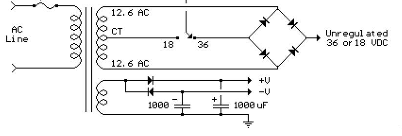
During the building we discovered we needed 2 input sources, one to deliver a positive voltage and the other to deliver a negative voltage. This was one set back in designing to use two voltage sources to power a single component, as no customer will accept to buy such a component. Our project only deals with the regulating of  the voltage. The regulator needs two input. If our project was to be considered in a large scale we will consider using a transformer. The transformer that will be suitable to use is a transformer with two secondary windings as shown below,


Figure 8: Transformer with two secondary windings

From  figure 8 above, we have 3 output which are; the unregulated VDC, the positive and negative for the op-amp. We can see that instead of using two input voltages, we can just use this transformer to replace them. 
  Another issue discovered was the heating of the pass transistor. The heat dissipated was reduced by adding a large resistor at the load. However, if a smaller load is to be used it is necessary to mount them on a suitable heat sink.  

Friday, 15 February 2013

Designing Stage

In the LAB we built our circuit design as shown in our previous update on a SK10 board, the circuit worked perfectly. However we discovered it was not going below 4V when we vary the transistor R12, so we had to go back to the circuit to know where the problem came from. The circuit was then adjusted to obtain a voltage  below 4V and even up to 0.1V. Below is the edited circuit diagram and  the output waveform.


Figure 6: The new Design


Figure 7: Output from the new design.

The output of the new design when compared to that of the older design is better. The two extra voltages provide bipolar voltages to drive the operational amplifier. The negative voltage is used to generate a reference voltage below ground so that the output can be adjusted down to zero.

Thursday, 31 January 2013

POWER SUPPLY
power supply is a device that supplies electric power to an electrical load. The power supply is needed for our everyday use to charge phones, laptops, to operate every electronic device. There are different circuit diagrams for supplying power. The process of supplying power is divided into four main part which includes, 


  1. Transformers
  2. Rectifiers
  3. Smoothing
  4. Regulating
The general block diagram of a regulated power  supply is shown in the diagram below 


Figure 1: Power supply block diagram

However we are concerned about designing and building the regulatory aspect of the power supply. Below is the designed circuit diagram for the voltage regulation and its simulations.


Figure 2: proposed power regulator


The above circuit contains two voltage sources, one is an AC while the other is a DC. In this design we are assuming that the voltage from the smoothing capacitor still contains ripples. That is why we have an AC supply from the signal generator. 
          The operational amplifier  uses the negative voltage of the input signal to generate a reference voltage below ground so that the output voltage can be adjusted. The current limiting is accomplished by sensing the voltage drop across a small resistor placed in series with the negative supply line. The output of the Op-Amp reduces the voltage at the base of transistor Q3 in figure 2 which in turn reduces the current to pass transistor Q1 so that the current stays constant. Transistor Q1 and Q2 should be mounted on a heat sink. 
          The output voltage (voltage across R15) depends on the value of the R12 resistor. The resistor R12 should be above 3.3K ohms to obtain a good output voltage. It should be noted that the higher the value of R12, the lower the output voltage. Below are the simulated waveform's for the  AC source signal,  input signal and the output signal.


Figure 3: The AC source signal with amplitude of 1V and frequency of 25hertz.


Figure 4 :The total  input signal from both the AC source and DC source with of  25V and internal resistance 1 ohm.


 Figure 5: The output signal.

From the above simulated waveform's, it can be seen that the circuit design worked properly and there was no ripple on the output.

The next update on this project will try to implement the above design into real practice. Watch out for it.